
Little Known Facts About Common causes and prevention of PCB Shortages – And Why They Matter
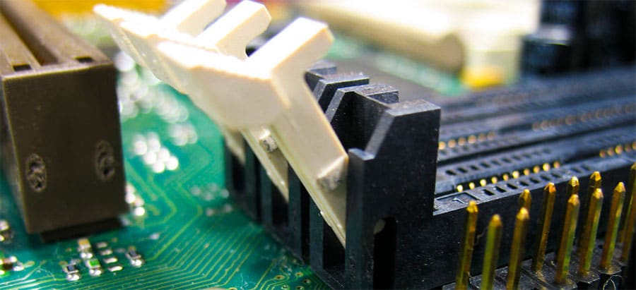
In PCB designing, it is crucial to understand just how PCB shorts occur, to minimize the occurrences. There are of course several causes of PCB shortages.
1. Contamination and Etching
Contamination comes in many different forms, none of which is good for your PCB. Cleaning may leave residues and films on the surface of your PCB. The dirt gets in between laminates or in between the layers of copper inside the PCB. This eventually causes the degradation and residual damage of the board. This can subsequently lead to short-circuiting of the board.
Conductive or metallic salts present in the PCB layers causes them to develop filaments called Conductive Anodic Filamentation. The filaments create shorts via non -conductive components of the multilayer PCB board. Copper dendrites form due to electrochemical etching and occur mostly due to board contamination by ionic mixtures and acids. When stripped wires go into the connectors, contamination shorts occur.
2. Safety with solder paste and checking stencil mismatch
Once built, the positioning of the PCB’s materials happens before the board goes into an oven. In the reflow oven, the solder paste on the board melts and becomes the connection from that particular component to the PCB. If in the wrong position, or if it even shifted positions a bit, the leads may mismatch with the relevant pads. The leads might connect to the adjacent pads. The leads may also be so close that the solder flowing back may cause a bridge to build between the leads.
If the stencil you use to apply the solder has holes whose sizes are a mismatch to the PCB pad size, then it creates a problem. If they are big, the solder will overflow to adjacent pads and if they are too small, the solder will not form a strong enough connection.
3. Reduce overcrowding
The size of components is reducing every day. The result of this is tinier pad sizes and more density in components. With more density in components, there is more threat of damage from heat and part interference. This means that if you need to re-do the design at a later date, the component density stands the chance of increasing costs and time
Your component pad size does not cause shorts directly on the PCB, but the smaller pads definitely make the shorts possible. Smaller pads have a smaller margin than the larger ones, meaning you have less protection when issues on layout occur. If the pads are big in comparison to the space in between, you will have solder bridges that form over that space. Solder bridges cause as much as 15% of PCB faults. This also means you cannot make larger pads in order to get some negotiating space for alignment.
Layout Issues
Having a smaller component pad makes it hard to chart traces. Traces get smaller and more tightly packed and trace routing has a big impact on the solder joint quality. True routing depends on:
- Trace connection width in relation to the pad
- The connections per pad
- Size of the pad
- Size consistency between various pads
High trace density areas are likely to have problems. There is the likelihood of solder bridges that create short circuits, less solder that creates gaps on the pad, and skewed components where the solder’s distribution isn’t uniform.
Take care of your PCB layout to prevent the risks of PCB shortage and failure by choosing software with many capabilities.
Have you read?
Biz 1on1 makes entrepreneurs the stars!
Family Businesses: A Promising Niche.
What Do Millennials Need? It’s All About Trust.
World’s Best Luxury Hotels For 2018.
Add CEOWORLD magazine to your Google News feed.
Follow CEOWORLD magazine headlines on: Google News, LinkedIn, Twitter, and Facebook.
This report/news/ranking/statistics has been prepared only for general guidance on matters of interest and does not constitute professional advice. You should not act upon the information contained in this publication without obtaining specific professional advice. No representation or warranty (express or implied) is given as to the accuracy or completeness of the information contained in this publication, and, to the extent permitted by law, CEOWORLD magazine does not accept or assume any liability, responsibility or duty of care for any consequences of you or anyone else acting, or refraining to act, in reliance on the information contained in this publication or for any decision based on it.
Copyright 2024 The CEOWORLD magazine. All rights reserved. This material (and any extract from it) must not be copied, redistributed or placed on any website, without CEOWORLD magazine' prior written consent. For media queries, please contact: info@ceoworld.biz
SUBSCRIBE NEWSLETTER